Tuesday, December 18, 2012

It's Alive! HV DC Supply is Fully Functional

After roughly half a year of design and troubleshooting, I finished fully testing my custom variable high voltage DC power supply yesterday. The supply is capable of producing up to 20 kV at 10 mA. I will be using it to charge my high-voltage capacitor bank and hopefully explode some water.

The finished and tested circuit
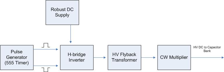
The circuit is essentially comprised of three subsystems: a DC mains supply, an H-bridge inverter, and a high-voltage multiplying rectifier. The first is visible in the top portion of the above photo. It's just your basic diode bridge rectifier, with a 60 Vp sinusoidal input and nearly 1000 uF of smoothing capacitance.

The H-bridge inverter can be seen in the middle of the photo. Its driving frequency can be varied between discreet values ranging from 40 to 47 kHz using the rotary switch visible towards the bottom of the shot. This small range of driving frequencies corresponds to a large range of output voltages (from about 8 to 20 kV), as my flyback transformer (not visible in the above photo) resonates at near 60 kHz. This phenomenon is illustrated below:

Above resonance


At resonance

Below resonance


The circuit's business end, the high voltage output stage, is depicted below:

Parts are (from left): flyback transformer, Crockoft Walton multiplier, protective diodes, output resistors

In order to prevent arcing between and within the high-voltage components, I had to submerge them all in mineral oil. While messy, this method was extremely effective at insulating the parts.

The small, innocuous-looking flyback transformer I used in my circuit is somewhat unconventional. Most HV hobbyists think of the large suction-cup sporting flyback transformers found in CRT's when they hear the term (see picture below). These transformers are frequently used to make spark generators and are easy to salvage from old TV's and computer monitors. They are generally much beefier than the downsized flyback I used in my supply, and one would expect to get more voltage from them.  I experimented with using one of these in my supply, but ultimately decided against it. All such flyback transformers I found were internally rectified (AC flybacks were outmoded in TV's thirty years ago) and therefore could not be used with my CW multiplying rectifier. So despite the traditional flyback's heft, I was able to get a greater voltage output from my miniaturized version by tacking a voltage multiplier onto its AC output.  

A classic flyback transformer, salvaged from an old computer monitor


Troubleshooting my circuit was hardly mundane; between prototypes, my circuit experienced some catastrophic failures. The aftermath of one is pictured below:


Casualties: four power transistors, one LCM555 timer, one breadboard
I was testing the circuit at the limits of its operating range, and I neglected to account for the heat my driving transistors would accrue. After operating for about five seconds, the transistors promptly burst into flames. Let it be known: the large heatsinks visible in the first picture are there for a reason!

Assuming my circuit doesn't spontaneously combust again any time in the near future, I will be using it to (carefully!) charge up some gargantuan high-voltage oil filled capacitors (see below). Once I'm confident  I can charge and discharge these monsters safely, I'll hook up my makeshift water accelerator barrel, and we'll see if I can replicate Peter Graneau's overunity water arc explosions.


Thursday, October 18, 2012

Back to the Drawing Board: Making my own High Voltage Supply

Don't think I've been spending all that time since my last post idly!

That couldn't be farther from the truth. These past 6 months I've been laboring over a little circuit of mine, a custom high voltage power supply that should be able to source all the power I need to blow up some water. The power supply is built entirely from scratch and took a lot of troubleshooting to get working. And, it's not quite done yet, but its completion is in sight.

I will elaborate on the circuit later when the designs have finalized and thoroughly tested.

The system's components are outlined below (click for larger image):


Finally, some quick snapshots of the physical circuit:

Custom DC supply (from 120V mains):
110-90V tapped mains transformer

High-current 120 Vp rectifier, with about 500 uF of smoothing capacitance 

Pulse generator and H-bridge inverter:

The 555 timer is visible towards the far left of the breadboard.
The rear MOSFETS drive the H-bridge transistors in the foreground
Below is a little demo of the H-bridge's operating principle:


Flyback transformers:

A small, non-standard HV flyback, rated at 9 kV. Feeds into the CW multiplying rectifier pictured later.
A more traditional HV flyback, salvaged from an old CRT. Output is rectified internally.

CW voltage multiplying rectifiers:

Uses low ESL "doorknob" capacitors. DC output is nominally four times the AC input.


Sunday, February 26, 2012

First Setup: No Success Yet

I have finally constructed and tested my planned version of the charging and discharging circuits. Unfortunately, I haven't gotten the circuit working properly; the circuit is functional, but can't induce a water explosion.

Below is a picture of my implementation of the charging circuit.

  
The leftmost breadboard holds the switching and control circuit. The silver box to its right is a  high-voltage neon sign inverter; it takes in 12 VDC and puts out 2 kV @ 60 kHz. The inverter powers a rectifying voltage multiplier (on the second breadboard). The circuit essentially consists of several Greinacher voltage doublers (described in the previous post) stacked on top of each other. The circuit is commonly known as a Cockroft-Walton (CW) voltage multiplier. It is named after physicists John Cockroft and Ernest Walton, who discovered the circuit in 1932 and used it to power their atom smasher. At no load, the output voltage is theoretically twice the peak input voltage times the number of Greinacher stages in the circuit. A simple two stage CW multiplier is shown below. If, for example, the circuit was powered by a 3 kVp AC source, the open-circuit output would theoretically be 12 kV DC.


The actual output is significantly less than the theoretical output, and decreases with increasing load current. The 5-stage CW multiplier used in my charging circuit should theoretically produce 30 kV at no load; the actual output is a little more than 10 kV.

The CW multiplier is connected through two 25 MOhm resistors to two special reed relays at the far right of the picture. The relays are each rated at 5 kV and are used to connect the charging circuit to the capacitor bank. 

The whole apparatus is mounted on top of a sealable plastic container lined with tin foil. Inside the container are the capacitor bank and discharge switching mechanism.


The plastic bin serves to insulate the capacitor bank from the circuit's operator. The tin foil lining is meant to act as a Farady cage. The capacitor bank's discharge is often accompanied by some arcing near the switching mechanism's electrodes; the tin foil Farady cage is there to neutralize the electromagnetic field generated by the arcs. This prevents the radio noise from interfering with oscilloscope measurements.

The obscure "switching mechanism" I referenced in the previous paragraph has consisted of two different devices over the course of this project. The first is a system of relays similar to the big red ones used in the charging circuit. These relays are switched manually when the voltage across the capacitor bank reaches the desired level. The second switching device is a much cruder spark-gap switch that breaks down at a certain voltage, determined (partly) by the spark gap's length (as well as by electrode shape, air moisture, and a slew of other factors). The former switching mechanism was eventually replaced by the latter because the relays didn't handle the capacitors' high-current discharges very well (to say the least: they may or may not still work).

I've also experimented with a couple different types of capacitors. The picture below shows a high-voltage "slapper" capacitor, rated at 15 kV with a maximum underdampened discharge current of >2 kA (yikes!). The capacitor is discharged using the spark gap switch described above.


When the discharge switch is closed, the capacitor bank is discharged through the water accelerator barrel. The accelerator is shown below, in actual and diagrammatic representation:


The accelerator's actual dimension turned out to be a lot smaller than those given in the diagram. Instead of 12 cm x 9 cm, the accelerator is approximately 5 cm x 3 cm. It's built from a couple of sections of 1/2" PVC pipe, a length of 6 AWG wire, and a 1 mm-thick aluminum sheet. It can hold up to 2 mL of water. 

During a discharge event, the voltage across the capacitor bank is measured using a specialty high-voltage voltmeter probe. The thing (pictured below) looks like it belongs on a Star Trek set, but it gets the job done. It has a 1000:1 attenuation ratio and an input impedance of 1 GOhm.


The discharge current is measured using a special current transformer, called a Rogowski coil, and an oscilloscope. The Rogowski coil produces an output voltage proportional to the rate of change of current through the wire it's wrapped around. To glean information about the current through the wire,  you can slap an integrator circuit on the end of your coil, or employ some other method of numerical integration.

During a discharge event, the coil voltage usually looks something like this:


This waveform is from the discharge of my 6 kV 0.3 uF capacitor bank. The spike seen towards the end of the waveform is an illustration of the effects arc-generated radio noise have on oscilloscope measurements. From the waveform, the derivative of the discharge current dI/dt can be modeled as follows:


where Io is a placeholder value for the initial current (in this case it is actually a quantity in volts taken from the oscilloscope readout), tau is the discharge time constant (approximately one fifth the pulse width, in seconds), omega = 2*pi*f is the angular ringing frequency (with f, the ringing frequency, in hertz), and t is time, in seconds. Integrating yields:


It's assumed here that the constant of integration is zero. If you want to double check this answer, I'll let you do the integration by parts yourself. Note that the proportionality constant of the Rogowski coil is negative, so it will flip the signs of the current waveform around. The above equation describes a waveform shaped similarly to the one seen in the oscilloscope screenshot. This derived equation for I(t) will be used to describe the current waveforms of discharges during this experiment.

In the case of the waveform shown above, Io = 24.6 V, tau = 56 uS/5 = 11.2 uS, f = 192 kHz, and omega = 2*pi*192 kHz = 1206 kHz. I(t) is minimized on the interval [0, inf) when t = 0, so the maximum discharge current will be the current at I(0). From our model for the Rogowski coil output, I(0) is:


Note that this quantity is in volt-seconds. Since the proportionality constant of our Rogowski coil is -1.1758 x 10^(-8) ohm-seconds, the actual discharge current is:


that is, 1.7 kA. Apparently, this isn't quite enough current to get any water to explode. To rectify this, I'm planning on revamping my charging circuit to increase the capacitor charging voltage (more power!). This should help increase the peak discharge current.

The results of my second attempt at the water explosion apparatus will be posted here shortly.    


Monday, January 2, 2012

Discharge Circuit Design

My latest work on the project has centered around the assembly and testing of my charging and discharging circuits. Below is a diagram of the circuit I ultimately implemented for charging and discharging my capacitor bank (click for larger resolution).


When the DPST mechanical switch S1 is thrown to the left, the leftmost DPDT relay S2 is actuated. This then turns the step-up converter on and actuates the SPST charging relay S3. The capacitor C towards the bottom right of the diagram is then charged to the converter's output voltage (approx 6 kV) through the 1.2M resistor. Once the capacitor is fully charged (if C = 0.3 uF, RC = .36 s and the capacitor C will be charged to within 1% of its charging voltage in 5RC = 1.8 s), S1 is thrown to the right, actuating the SPST discharging relay S4 and shorting the capacitor's positive plate to ground. The resultant pulse discharge can be used to initiate a water arc explosion.


The diodes in parallel with each relay are there to protect the switch S1 (and the contacts of relay S2) from the momentary voltage spike produced when the relays are switched off. Relays S3 and S4 must be specially made for switching HV signals. I used two 5kV reed relays connected in series for both S3 and S4. The reed relays are designed so that their contacts are contained in an evacuated chamber, thus allowing them to switch high voltage without sparks arcing between the contacts.


The box labeled "DC-AC-DC Step-Up Converter" will likely comprise the below circuit.


The unit after the step-up inverter is called a Greinacher voltage doubler; it takes an AC signal and outputs DC (with ripple) at twice the peak input voltage. The first capacitor is charged on the negative half of the AC  cycle to the AC peak voltage. On the positive half, the output is a superposition of the input AC waveform onto the capacitor's discharge current. The second capacitor reduces voltage ripple.

The circuit's open-circuit output is nominally 2Vp. Under load, the circuit's output voltage drops with load impedance. The circuit's exact voltage characteristics are given by
Where I(load) is the current through the load (A), f is the frequency of the AC input (Hz), and C is the capacitance of the doubling capacitor (F). Assuming a maximum load current of 6kV/1.2MOhm = 5 mA, an input frequency of 60 kHz, and an input capacitance of 270 pF, the circuit's minimum output voltage comes out as 5691.4 V. As the capacitor C charges, I(load) will decay to zero, and the output voltage will level off at 6 kV.

Saturday, December 3, 2011

Design and Testing for the Discharge Apparatus

My apologies for the lateness of this post. The lack of activity was not due to ennui, but to school, homework, band practice, and other things that have been keeping me from the project. Science fair is fast approaching though (only three more months!), so starting now, I am officially moving into project work mode.

Since I last posted, I've made some considerable revision to the charging and discharging circuit plans based on practical constraints and the ratings of my components. First off, I was unable to find any capacitors in the 1 uF range rated at more than 600 volts, so I settled for a pack of eighteen 0.1 uF 3kV polypropylene caps. In any configuration, a bank comprising all eighteen of these capacitors can safely store a maximum of 8.1 J without risk of breakdown (you can check the math). This is about 20% the energy reported to have been stored in P. Graneau's bank during his experiments. However, Graneau's research shows that cold fog explosions are highly current dependent, so I'm hoping that as long as I can get enough current flowing (i.e. as long as I can get the voltage across my capacitor bank high enough), I can still generate some impressive explosions even with my (relatively) small capacitor bank.

My caps' lower-than-expected voltage rating forced me to downsize some of the components in my charging circuit. Most notably, my 16 kV power supply had to be rebuilt so that its output wouldn't punch big gaping holes through my capacitors. The supply was put together from a 12 VDC wall adapter, a 2000V neon sign inverter, and a five-stage CW multiplier to step up and rectify the inverter's output. I swapped out the 12 volt wall adapter for a 7.5 volt one and chopped three stages off the multiplier to lower the supply's output to around 4.7 kV. The power supply is shown below, along with a couple of the polypropylene caps and a switching relay.


While this should have been suitable for charging any bank made from parallel units of two or more series capacitors, lowering the input voltage made the supply a bit finicky (maybe because inverter was current limited). The supply's output voltage would vary with load resistance; large loads (on the order of a couple megohms)corresponded to normal output voltages (of around 4.7 kV), but smaller loads (down to 500k ohms) would yield lower output voltages (down to around 1 kV). The output would drop to 0 for loads of less than 500k (probably because of the current limiter).

Needless to say, working with such a mercurial supply is undesirable. So, I scrapped it, and ordered a 1.5 kV non-limited inverter (http://www.amazing1.com/hv-dc-power-supplies.htm) to build a new supply from. I'll be able to stick a voltage multiplier on the end of it to step up the output to 3 kV, 6 kV, 9 kV, or whatever is needed. The inverter should be here any day now.

Despite its poor operational characteristics, I was able to use the old power supply to test some other components of the discharging system, namely, my measurement and switching circuits.

Depicted below is a rectifying circuit I threw together to test my measurement system:


On the left, I'm running 120 Vrms @ 60Hz into the transformers, and they're outputting a 60 Vrms sinusoid. On the breadboard, you've got your standard diode bridge rectifier, without voltage regulation. The rectifier produces an 80 VDC signal, with negligible ripple current. I'm using that to charge the shown capacitor (an electrolytic I scrapped from an old HV supply's rectifying circuit). At the far right of the screen, you can see my homemade Rogowski coil (yes, that is a clothespin holding it closed) ready and waiting to capture the discharge current resultant when I flick the switch and short the capacitor's leads to each other.

Wikipedia has a nice article here on the theory behind Rogowski coils. In essence, they're current transformers whose secondary winding produces an voltage proportional to the rate of change of current through the primary winding. My particular coil has a proportionality constant of -1.1785*10^(-8) ohm-seconds. So unfortunately, I wasn't able to get a reading from it when discharging the cap in this configuration; the discharge current was just too small to produce a measurable voltage in the coil.

Switching to the setup shown in the first pic, however, yielded coil outputs that looked something like this:


When I first saw this readout, I grew wary of my coil's accuracy. When looking at the voltage across a discharging a capacitor, one would expect to see a nice RC time constant-esque exponential decay sort of function, not the oscillating wave-packet looking thing shown above. My first thought was that RF noise must be contaminating the signal. Substantial arcing was evident around the relay contacts during discharge; perhaps the coil was picking up the momentary radio noise generated by the sparks, rendering the actual signal indiscernible and accounting for the odd prominence of the sinusoid seen above.

I soon realized that there were several problems with this theory, however. Firstly, the trace shown above was very easy to duplicate, and did not seem to vary heavily with changes in the capacitors' charge time or charging voltage. A transient RF signal should have behaved much more erratically; it seemed unlikely that any such signal would exhibit so much consistency.
Secondly, upon closer inspection of the waveform, it was apparent that the large ≈800 kHz signals were further corrupted by a less obvious, more irregular 20 MHz signal of varying amplitude. This signal would peter out after about 7.5 us, 2.5 us before the end of the discharge event. Due to its higher frequency and lower repeatability, it seemed more likely that this was the radio signal produced by the arcing around the relay. I was then left at a loss for an explanation for the source of my original signal.

After reviewing some literature, I eventually arrived at the conclusion that the signals I was obtaining were actually accurate reflections of the current-flow in my discharge circuit. It turns out that in high voltage, low resistance RC circuits, actual circuit operation tends to deviate significantly from the theoretical. Larger capacitors have a tendency to ring when charged to a high voltage and discharged quickly; when a high-voltage capacitor is discharged through a small resistance, a large current rushes from the more positive plate to the more negative one, which pulls the negative plate below ground and places a negative voltage across the capacitor. Current then rushes back from the more negative plate to the more positive one, which in turn swings the voltage across the cap positive again. The discharge current oscillates back and forth in this manner until the ringing voltage eventually decays to zero and discharge ceases.

The only real way to test the accuracy of this theory was to erect a radio-shield around the relay and see if the Rogowski coil's output was affected. But, before I could do that, I had to devise a way to charge and discharge my capacitors safely.

Ideally, I would switch my charging and discharging circuits a simple SPDT mechanical switch. When the switch was in one state, the charging circuit would be closed and the discharging circuit would be open. When the switch was in the other, the charging circuit would be open and the discharging circuit would be closed (note: this ensures that the charging and discharging circuits can never both be closed simultaneously). Of course, the actual switching mechanism must involve more than just an SPDT switch, as I would want to be able to switch my capacitor bank remotely without having to deal directly with the high-power charging and discharging circuits.  

Obviously, no transistor could take on the daunting task of switching a 3 kV signal. So, I resorted to using relays, like the one depicted earlier, to switch the charging and discharging circuits. In the end I had access to three of them, and unfortunately, the three had different default states: the two smaller ones defaulted open, and the bigger one defaulted closed. Neither of the smaller relays could switch a 3 kV signal on their own, so they had to be used together as a single relay with higher inductance and voltage ratings. This made the simple two-state switching circuit (with each state of corresponding to the actuation of one of the two relay groups) impossible, and forced me to employ more creative methods to get the relays to switch when I wanted them to.

Depicted below is one idea I had for such a circuit, employing a simple transistor NOT gate and some small, high-power resistors. The diode across the second inductor is there to protect the transistor from the momentary high voltage produced when the transistor is switched on and the inductor tries to keep a current flowing through it. Also note that the single relay on the left really represents two relays in series.


When the SPDT switch is in its neutral state, the first relay is off, and the second relay is on; both the charging and discharging circuits are open. When the switch is in its low position, the first relay is actuated. Now, both relays are on; the charging circuit is closed, and the discharging circuit is open. When the switch is in it's high position, the transistor is switched on, and current virtually stops flowing through the second relay. Now, the first relay is off, and the second is on; the charging circuit is open, and the discharging circuit is closed.

Another much simpler alternative is shown below.


The symbol immediately downstream of the voltage source is a break-contact switch. In its default position, both relays are on; the charging circuit is closed, and the discharging circuit is open. When the switch is opened, current stops flowing to the relays, and they shut off; now, the charging circuit is open, and the discharging circuit is open.

The video below is a demonstration of the above circuit in action, with a couple of LEDs as replacements for the loads of the charging and discharging circuits.


After additional testing, I found that the circuit also handles HV switching quite well. I should be able to use it when putting together the final discharging circuit.

Wednesday, June 15, 2011

Design Plans

Here are a couple of diagrams and schematics giving a general outline of the experimental apparatus. None of the devices described in the diagrams have been built yet, as I am still looking for the materials necessary for their construction.

This first image is a circuit diagram for discharge circuit (click for larger resolution):

As you can see, the design is relatively straight-forward; it's just a basic circuit for capacitor charging and discharging. With the switch S open, the capacitor bank is charged to the input voltage (which depends on R1 and R2; I plan to set the voltage divider ratio at around 3/4, giving an output of 12 kV with a 16 kV source). In actuality, there will probably be a balancing resistor placed across each capacitor to avoid dangerous fluctuations in the capacitor voltages due to leakage currents. The value of each capacitor should be about 0.18 uF, which makes the total capacitance of the bank about 0.55 uF. After charging, the voltage source is removed and the switch S is closed, initiating the capacitor discharge. No resistors or inductors will be placed in the actual discharge circuit; the lumped values Rc and L represent the distributed circuit resistance and inductance, respectively. Essentially, closing the switch S shorts the circuit, so as to maximize the discharge current.

The next several diagrams are devoted to outlining what exactly is going to be placed in the ambiguous "water arc chamber" box. There will likely be three different accelerator designs used during this project. The first will be used to measure the kinetic energy of the water explosions, and is modeled after P. Graneau's accelerator designs.
(All the following diagrams are cross-sectional; the actual accelerators will be cylindrical.)
The purpose of the secondary projectile is to allow for the measurement of the fog jet's mass and velocity, which can be used to approximate the explosion's kinetic energy. The energy contained in the electrical impulse initiating the explosion will also be measured, using an electrostatic voltmeter to measure the voltage across the capacitor bank and an oscilloscope with a Rogowski coil to measure the current flowing through the discharge circuit. The two values will be compared to determine approximately how much (if any) internal water energy is released in the fog explosion (both energies may vary with water purity, water salinity, water volume, input voltage, max current, pulse length, etc.)

If it is found that a significant amount of energy is released during the explosion process, a new chamber will be built to capture the kinetic energy of the fog and convert it to a more useful form (say, electricity). The following is a diagram of one possible such chamber.
This design uses a turbine generator to convert fog kinetic energy to mechanical energy to electrical energy. After the water passes through the turbine, it is pumped back to the explosion barrel to undergo the discharge process again. To increase the net output of such a system, numerous turbogenerator chambers may be hooked up in series, so that multiple water explosions can occur simultaneously, each induced by the same discharge current.

I am skeptical of the efficiency of such a design. Water arc explosions have only ever been achieved with very small amounts of water (about 3.4 mL), which are accelerated to very high velocities (in the range of 1000 m/s). I anticipate that a turbogenerator will not be able to handle such a small mass moving at such a high velocity very effectively.

An alternative may lie in MHD technologies, however. Below is a diagram of a possible MHD generator chamber design.
The idea behind this approach is that the water, after being ionized (or dissociated, atomized, etc.) by the electrical arc, will be sufficiently charged to serve as the conducting fluid in the generator. It may also be helpful to use saltwater as the fluid in this application, as it will be more conductive and increase the efficiency of the MHD generator. As with the turbogenerator design, multiple MHD generator chambers may be connected in series to increase the net output of the system.

Thursday, June 9, 2011

Project Start and Overview

In this blog I will be posting progress updates on my latest science project, which is an investigation into the feasibility of water arc explosions for power generation. The project has two main goals:

a) to reproduce the experimental results obtained by P. Graneau et al. in their research on water arc explosions (i.e. the findings that the kinetic energy of an electrically-induced fog explosion can exceed the electrical input energy)

b) to design and build an apparatus to convert the kinetic energy of such a water arc explosion into useful electrical energy, using either an array of conventional turbo generators or a variant MHD generator.

As of now I am still gathering materials and resources for the experimental apparatus. I will be able to post some design elements of the project (e.g. circuit diagrams) soon.